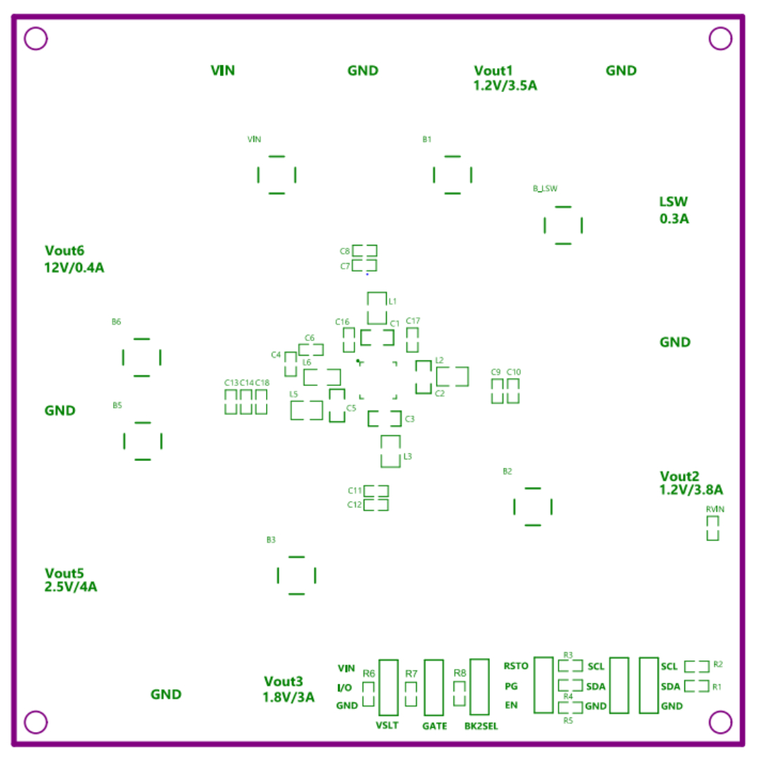
• Input Range: 2.6V to 5.5V
• 5 Independent Synchronous Bucks and 1 Independent 400mA Synchronous Boost, 1 Voltage Detector
- Buck1: Max. Current 3.5A (0.725 V to 1.825V, 6.25mV Step, Default on 1.2V)
- Buck2: Max. Current 3.8A (0.5 V to 1.2V, 6.25mV Step, Default on 1.2V)
- Buck3: Max. Current 3A (0.96V to 1.86 V, 7.5mV Step, Default on 1.8V)
- Buck5: Max. Current 4A (1.5 V to 2.75 V, 12.5mV Step, Default on 2.5 V)
- Boost6: Max. Current 0.4A (8 V to 15 V, 500mV Step, Default on 12 V)
- LSW: Max 300mA. Max. Ron 120mhom, Input Connect to VIN Internally, ON/OFF Controlled by I2C)
• I2C Interface up to 3.4MHz
• Independent PMIC Hardware Reset (Make all Channels Return to the Default Voltage)
• DVS (Dynamic Voltage Scaling) Controlled by I2C Interface
• Auto PWM/PFM Mode or Forced PWM Mode Controlled by I2C Interface
• Pull down Mode to Discharge all Channels Forcedly Controlled by I2C Interface
• Support to Adjustable Discharge Resister Controlled by I2C Interface
• Programmable the Various Function by OTP (Each Channel Start up Delay Time, RSTO Delay Time (Power On, RSTO Threshold)
• Enable Output Pin to Synchronous External Device Sequence
• Ultra-Fast Transient Response
• Support to Protection Function (Thermal Shutdown (Typ. 150˚C), Over Voltage Protection (External/Output), Over Current Protection, Over Load Protection)
• Input Voltage Monitor Function: Input Monitor bit will be Set from 0 to 1 when Input Exceeds Specific Value.
• Compact 5mm x 5mm QFN Package, 0.45mm pitch
• Green RoHS Package, Pb-Free Lead Finish, Halogen Free Mold Compound