150V, Dual Output Step-down Converter,
and Half Bridge Driver with Charge Pump
![]()
- Parameters
- Features
- Description
| Part number |
SQ37509VAQ |
| Driving FETs type |
|
| Channel(#) |
|
| Input bias voltage (V) |
7.5 |
| Output bias voltage (V) |
150 |
| Sink/Source current (A) |
3 |
| Features |
|
| Package |
QFN5×5-24 |
| Operating temperature range(°C) |
|
| Functional safety category |
|
- Wide Input Voltage Range: 7.5V-150V
- Dual Output Current Capability: VDD1 Buck1: Continuous 200mA @VDD1=12.5V 3V3 Buck2: Continuous 400mA / Pulsed 800mA
- Constant On-Time Control
- Switching Frequency VDD1 Buck1: Programmable 350 kHz~650 kHz 3V3 Buck2: Fixed 1MHz
- ±2% 3.3V Output Accuracy Over -40℃ to +125℃ Temperature Range
- Internal Soft-Start Limits Inrush Current
- High Source/Sink Current: 3A/3A
- CMOS/TTL Compatible Input Versions
- 5.7ns Rise and 4ns Fall Time with 1000pF
- Fast Propagation Delay Times
- 5ns Delay Matching
- Charge Pump Current capability: ≥25mA
- Compact package: QFN5x5-24
The SQ37509 is a dual-output Buck converter and highspeed half-bridge MOS driver with a charge pump function. The Buck converter operates over an input voltage range of 7.5V to 150V. The dual output can provide either 12.5V/200mA or 3.3V/400mA current capability. The SQ37509 integrates a high-voltage floating driver for directly driving high-side and low-side channels. The floating channel can drive a 150V N-channel MOSFET in a high-side configuration. The input logic level is compatible with standard CMOS or TTL. A charge pump circuit is utilized to ensure the complete turn-on of the high-side MOSFET. This device is available in a QFN5x5-24 package.
Evaluation Board
-
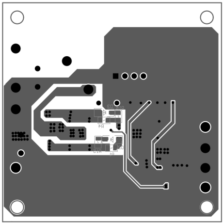
Photo of evaluation board
-
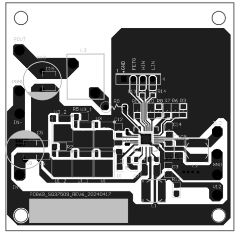
Photo of evaluation board
The EVB_SQ37509VAQ is intended for evaluating 150V, Dual Output Step-down Converter, and Half Bridge Driver with Charge Pump